INTRODUCTION:-
Today in this episode of Arduino projects I am going to introduce you with a new electronic circuit. This electronic circuit that I am going to introduce is known as 'Boost Converter' or 'Step-up Converter' or 'DC to DC Converter' or SMPS(switch mode power supply), it does not matter however you want to call it The job of this circuit is to Step up the low DC Voltage to a high DC voltage efficiently But there is a thing that you need to keep in your mind is that this circuit can only step up DC voltage not AC but in Case of AC voltage you can use a Step up transformer to step up the AC voltage but This is an another subject to discuss on The boost converter that I am going to design in this project or episode, operates on 4V - 5V DC and output voltage can be adjusted from 5V to 30V. You can adjust the output voltage according to your necessity But the second thing that you need to keep in your mind is that you can't connect a DC Load than draws more current.
In this Arduino project, I will introduce everyone to a crucial electronic circuit in power management systems: the "Boost Converter", also commonly known as a Step-up Converter or DC-to-DC Converter.
The primary function of this circuit is to efficiently increase a low DC voltage to a higher level, utilizing the principles of SMPS (Switch Mode Power Supply). It's important to note that this circuit is designed only for increasing DC voltage and cannot be used with AC current (for AC, we would use a transformer for step-up instead).
In this project, I have designed a Boost Converter that supports an input voltage range of 4V - 5V DC and can adjust the output voltage from 5V up to 30V DC according to application requirements. However, users must be aware that as the voltage increases, the current supplied will decrease according to the law of energy conservation. Therefore, high-current loads should not be connected beyond the circuit's limits.
HARDWARE LIST:-
To achieve an efficient and stable circuit, we need to use high-quality components as follows:
- ATTINY85 (8-BIT Microcontroller)
- IRF Z44 MOSFET(N-Channel)
- 1N5819 SCHOTTKY DIODE
- INDUCTOR(COIL)
- 8-PIN DIP IC SOCKET(HOLDER)
- SCREW TERMINAL
- DOUBLE SIDE PCB
- ELECTROLYTIC CAPACITOR
- RESISTORS
- ATTINY85 PROGRAMMING SHIELD
ATTINY85:-
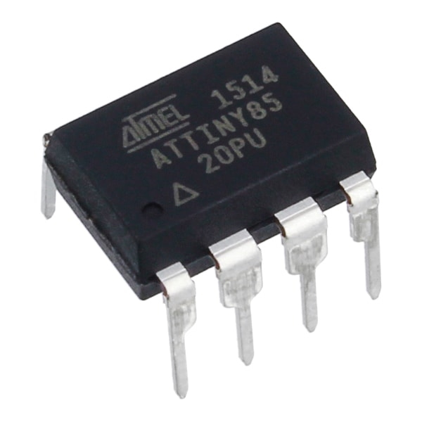
ATtiny85 is a high performance, low power 8-bit microcontroller based on Advanced RISC Architecture. It has 8 Kbytes of In-System Programmable Flash and is popular because of its compact size and its features.
Diving Deep into ATtiny85: The Tiny Brain
The ATtiny85 is a high-performance, low-power microcontroller from Microchip's (formerly Atmel) AVR family. It uses a RISC architecture and has 8 Kbytes of Flash memory. Despite its small 8-pin package, it has the capability to generate precise PWM signals and read Analog values accurately, making it ideal for space-constrained projects.
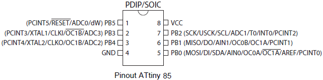
PIN-OUT OF ATTINY85:-
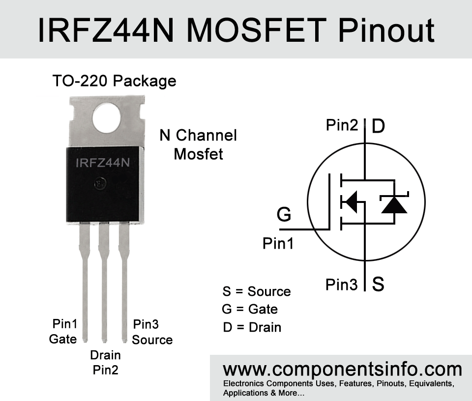
PIN-OUT OF IRF Z44(MOSFET)
WORKING PRINCIPLE:-
The working principle of the boost converter is similar to modern SMPS(switch mode power supply) so this is why a boost converter is also called a switch mode power supply or SMPS. To Explain the working the of the boost converter I am taking the help of the circuit given below.
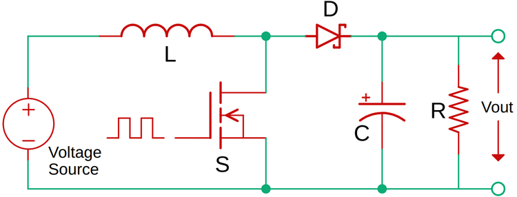
This electronic circuit consists of five passive electronic components-
- INDUCTOR(L)
- SWITCH(SW)
- SCHOTTKY DIODE(D)
- ELECTROLYTIC CAPACITOR(C)
- LOAD RESISTOR(R)
Vi is the input voltage for the circuit and for my circuit the input voltage ranges from 4V to 5V. Vout is the output voltage of the circuit.
The heart of a Boost Converter is energy management through switching, using five main components:
- Inductor (L): Stores energy.
- Switch (MOSFET): Controls current flow.
- Schottky Diode (D): Prevents reverse current and maintains voltage.
- Capacitor (C): Filters the output voltage to be smooth.
- Load (R): The end device.
WORKING THEORY:-
STEP 1:- When switch(SW) is closed(ON), the inductor(coil) comes in parallel with input voltage(Vi)and a small current suppose I starts flowing the magnitude of this current increases slowly slowly and after some time the value of I achieves its maximum value This increasing current creates an increasing magnetic flux(Changing Magnetic Flux) around the inductor and according TO first law of Faraday any change in magnetic Flux produces an induced EMF in the circuit(in this case an inductor).and once again according to the second law of Faraday the polarity of this Induced EMF is opposite to input Voltage(Vin).
Step 1 (Switch ON): When the MOSFET conducts (closes), the inductor is connected in parallel with the input power supply (Vi). Current begins to flow through the inductor, increasing steadily and creating a magnetic field to store energy. At this moment, the diode blocks current from flowing back from the output.
STEP 2:- When switch(SW) is closed(ON), capacitor C starts discharging through load resistor(R){While explaining the step1, I am assuming that capacitor C is already charged }when switch (SW) is ON load is capacitor C maintains the flow of Electric Energy in the Load resistor.
Step 2 (Capacitor Discharge): While the switch is ON, the energy supplied to the load comes from the capacitor (C) that was previously charged, to maintain a constant voltage.
STEP 3:- When switch(SW) is opened(OFF), the inductor L comes in Series with input voltage(Vi) and the polarity of the induced EMF across the inductor is opposite to input voltage(Vi) so total output Voltage(Vout) will be sum of input voltage(Vin) and induced EMF because in this step the input voltage and induced EMF behave just like two batteries in series This time capacitor C starts charging. and this time load resistor R is supplied by the sum of induced EMF and input voltage(Vin).
Step 3 (Switch OFF): When the MOSFET stops conducting (opens), the magnetic field in the inductor collapses rapidly, generating a reverse inductive voltage (Flyback Voltage) which adds to the input voltage (Vi). This causes the total voltage flowing through the diode to be greater than Vi. This energy then charges the capacitor and supplies the load.
STEP 4:- When switch(SW) is closed(ON) again, the inductor starts storing electrical energy in its magnetic field and load resistor is supplied by capacitor C and the rest theory of this part holds the same as STEP 1.
Step 4 (Repeat): This process repeats tens of thousands of times per second (High Frequency) to continuously maintain the output voltage higher than the input.
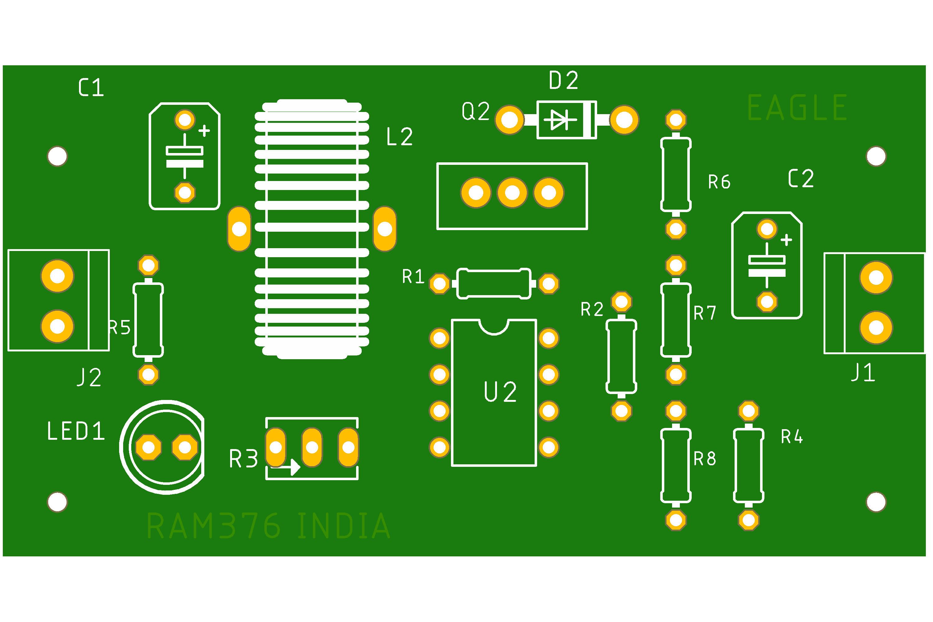
MAKING THE CIRUIT:-
During making the circuit you must have a temperature controlled Soldering Iron to adjust the temperature and all the devices that I am using here are THT(Through hole Technology) type. for soldering all the components I am using a double side PCB(printed circuit board) because the quality of the double side PCB is Excellent It is necessary that you must have good experience of soldering otherwise when you power your circuit first there may something blew up.
When assembling the circuit, a temperature-controlled soldering iron should be used because we are using a Double Sided PCB, which has better heat dissipation than usual. If the temperature is not high enough, it may result in incomplete solder joints (Cold Solder Joint). All selected components are THT (Through-hole Technology), which is easier for makers to assemble.
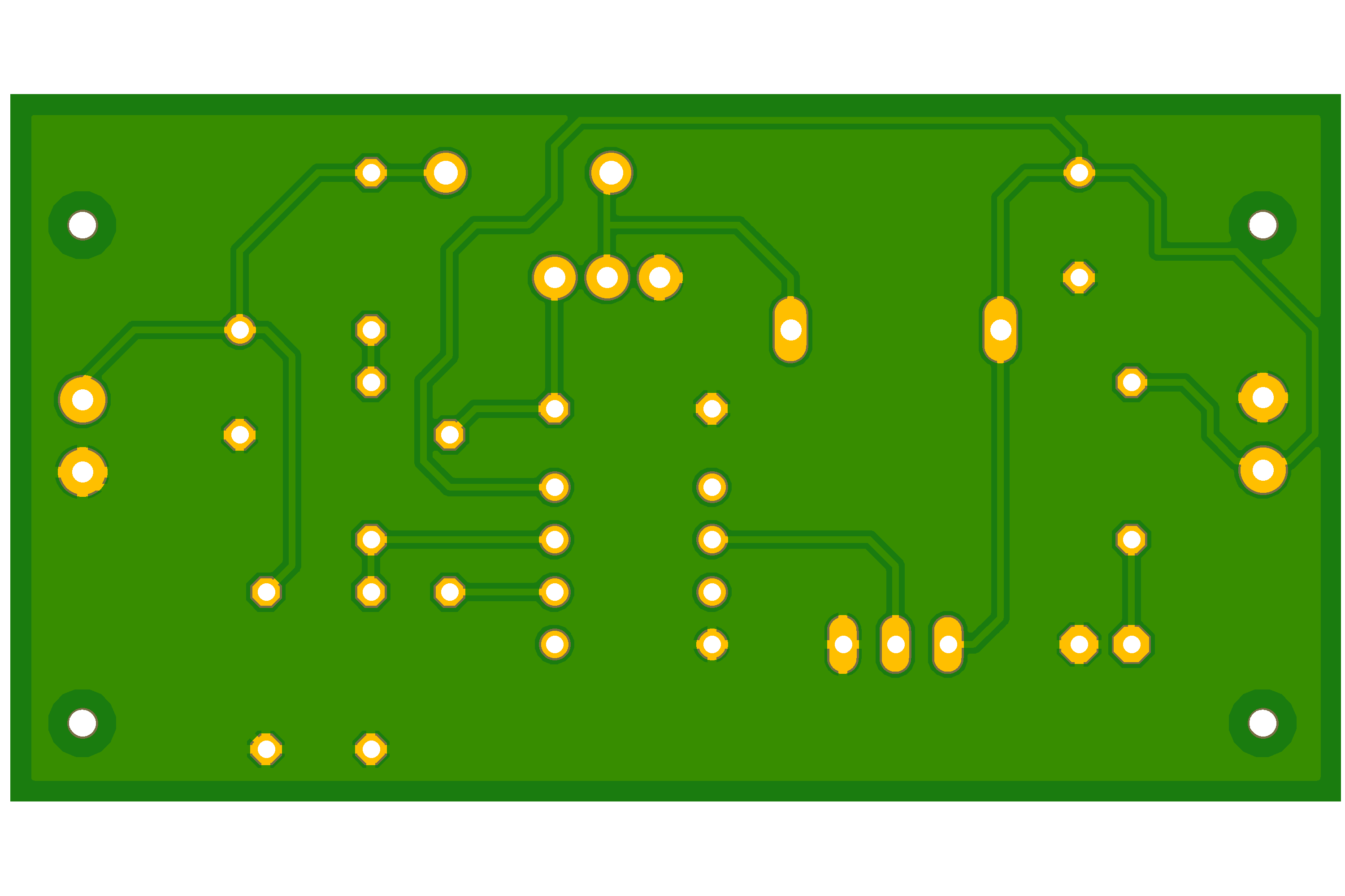
PICTURES OF MY WORK:-
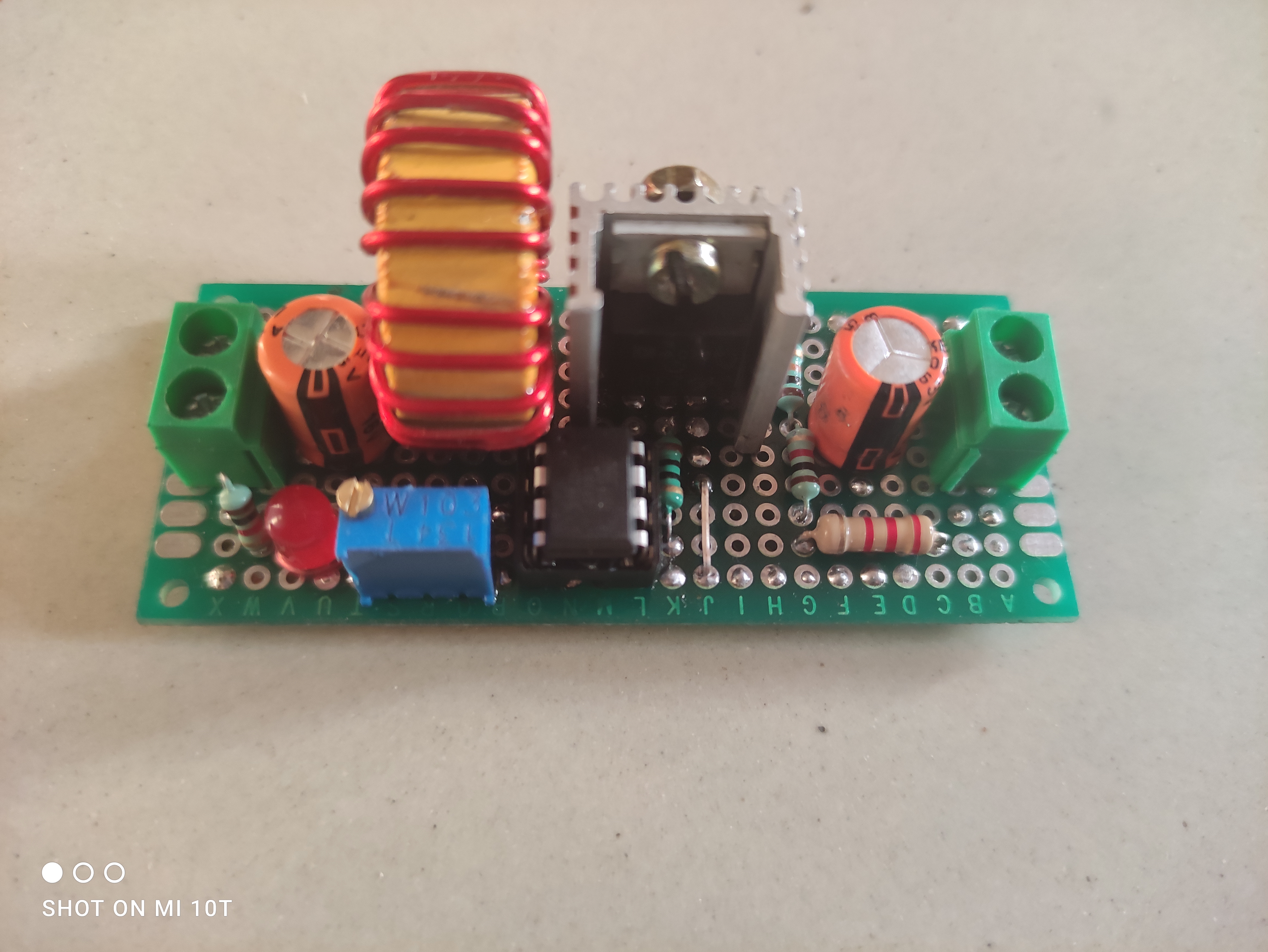
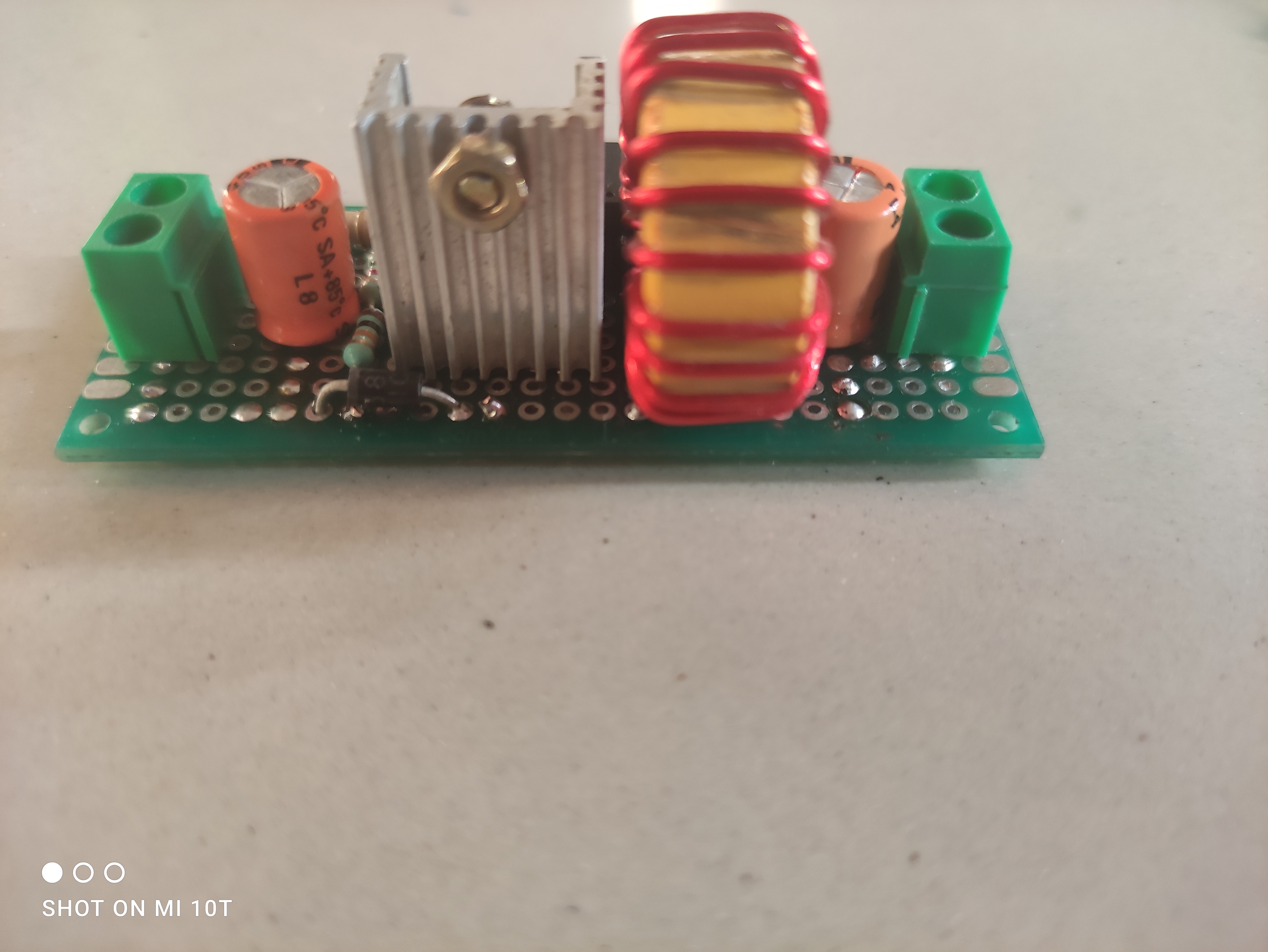
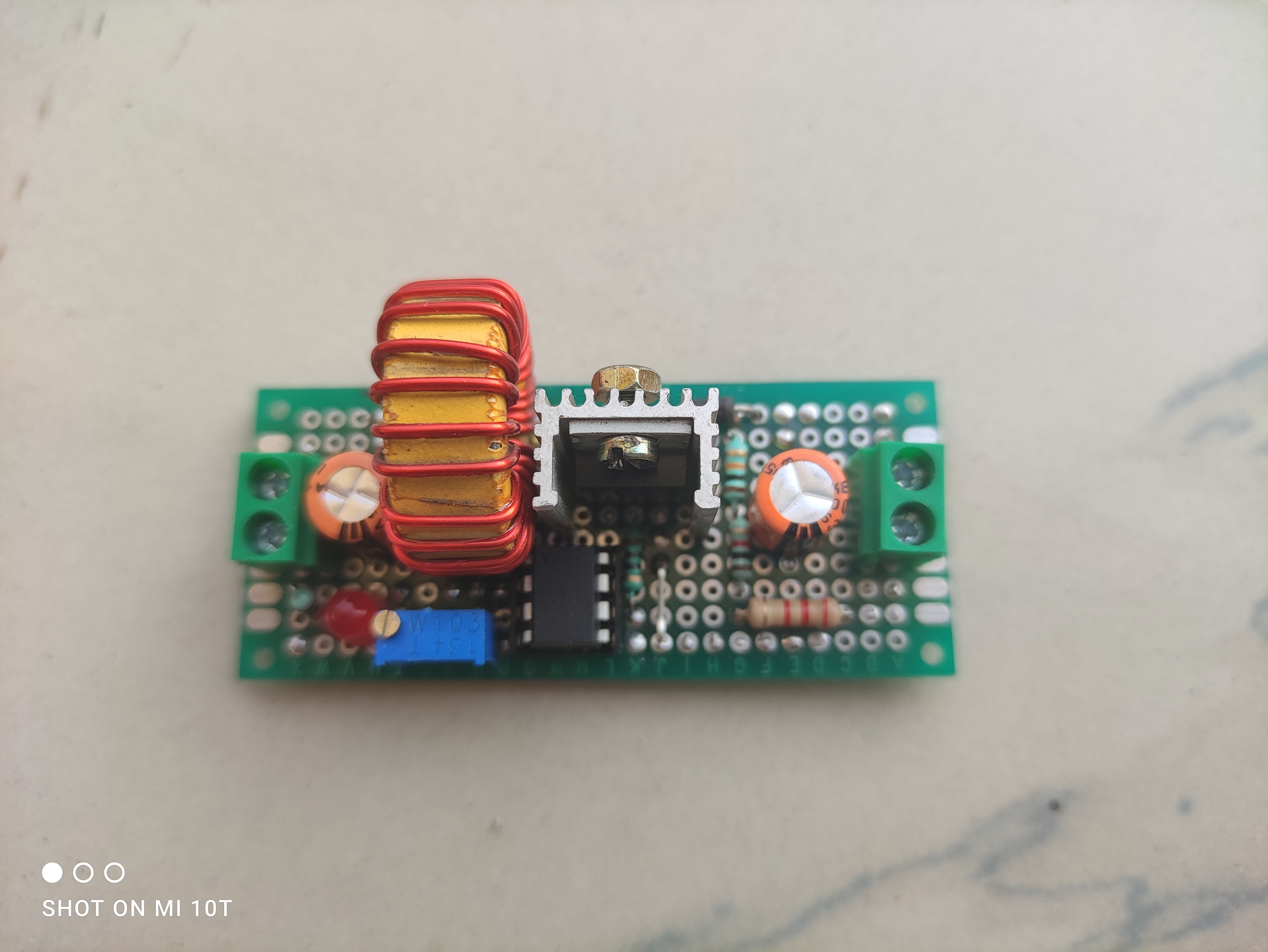
PICTURES OF THE PCB:
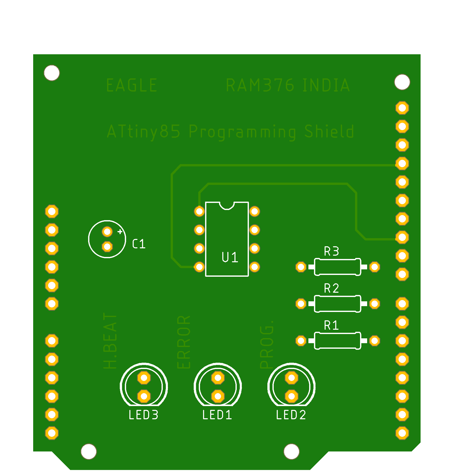
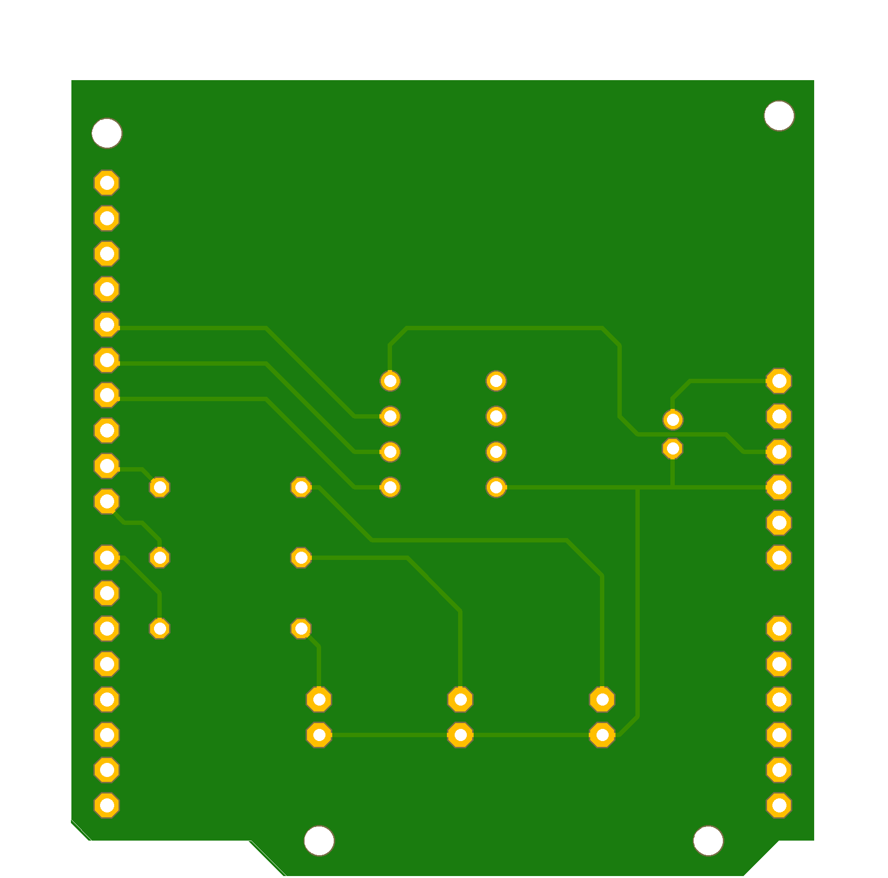
ATTINY85 PROGRAMMING SHIELD:
PROGRAMMING ATTINY85 USING ARDUINO UNO:
In order to Program the ATtiny85 microcontroller with with your Arduino IDE, first of all you need to install the ATtiny Boards in your Arduino Arduino. Follow the given steps in order to add ATtiny Boards in Your Arduino IDE-
- Step-1. Connect your computer or PC to internet and open the Arduino IDE software.
- Step-2. click on tools option of your Arduino editor and then choose Board>Board>Board Manager and finally click on Board manager and after opening the board manager successfully, type attiny and search for it, after few seconds you will see that an attiny library will appear on the board
- Step-3. Install this library by just clicking on install option and attiny boards will add in your Arduino IDE
- Step-4 now go on the home page of Arduino IDE and again click on tools > Board and you will see attiny board option in your arduino board option.
BURNING THE ATTINY85 BOOTLOADER ON ATTINY85 CHIP:
when you purchase a new ATtiny85 microcontroller from market or any online store, It comes without Bootloader. So you have to burn the ATTINY85 bootloader on your ATtiny85 Chip for this you can take help of my DIY ATtiny85 Programming shield and and Schematic diagram. I have given the Circuit diagram of DIY ATtiny85 shield so you can create your own DIY ATtiny85 Programming shield.
FOLLOW THE GIVEN STEPS TO BURN BOOTLOADER:
- Step-1 Connect the ATtiny85 Chip to Arduino UNO using jumper wires with the help of my schematic. after completing your wiring please make sure that you have connected each wire on its proper place other wise bootloader will not upload on the ATtiny85 chip.
- Step-2 Connect the arduino UNO to your computer or PC and upload the Arduino ISP sketch on the arduino UNO. you can get the Arduino ISP sketch from the examples. After successfully uploading the arduino ISP sketch on your arduino, now you are ready to burn the bootloader on ATtiny85.
- Step-3 Click on tools option and select Attiny Microcontrollers > ATtiny85> Processor>ATtiny85>Clock internal 8 MHz
- Step-4 Again click on tools > Programmer>Arduino as ISP
- Step-5 Now finally click on Burn Bootloader option and ATtiny85 Bootloader starts burning and after few second you will get a notification from Arduino IDE that Successfully burned the bootloader.
ATtiny85 Programming Steps
Before using the ATtiny85, we need to Burn Bootloader and Upload Code via Arduino UNO using the Arduino as ISP technique.
1. Preparing Arduino IDE:
- Go to
File > Preferencesand add the URL for ATtiny Boards in the Additional Boards Manager field. - Go to
Tools > Board > Boards Manager, search for "attiny", and click Install.
2. Burning the Bootloader:
Newly purchased chips usually do not have a Bootloader. We need to install it for the chip to operate at 8 MHz (Internal) frequency:
- Connect the ATtiny85 to the Arduino UNO according to the Programming Shield diagram.
- Select the
ArduinoISPexample sketch and upload it to the Arduino UNO. - Set
Tools > Board: ATtiny25/45/85andProcessor: ATtiny85. - Select
Clock: Internal 8 MHz. - Select
Programmer: Arduino as ISP. - Click "Burn Bootloader".
UPLOADING THE BOOST CONVERTER SKETCH:
After successfully uploading the bootloader, you are ready to upload the boost converter sketch on the ATtiny85 Chip. For this you should not have to change the previous setting that you make on arduino IDE while burning the bootloader. otherwise the sketch will not upload on the ATtiny85. open the boost converter sketch and click on sketch option and choose Uploading using Programmer and your boost converter sketch will successfully uploaded on ATtinu85. Now remove the ATtiny85 Chip from the programming shield and insert in into your boost converter PCB and and Enjoy Of your own Boost Converter.
SKETCH OF BOOST CONVERTER:
This code acts as a Closed-loop Feedback System controller to maintain a constant voltage level as adjusted by the Potentiometer.
#define F_CPU 8000000 // Defines CPU frequency at 8MHz
int pwm = 1;          // Output pin for sending PWM signal to MOSFET
int potinput = A2;    // Pin to read value from Potentiometer for desired voltage
int feedbackinput = A3; // Pin to read feedback voltage from Output

int potinputval;
int feedbackinputval;
int pwmval;

void setup() {
  // Sets Timer Registers to generate high-frequency PWM
  TCCR0A = 2 << COM0A0 | 2 << COM0B0 | 3 << WGM00;
  TCCR0B = 0 << WGM02 | 1 << CS00;
  TCCR1 = 0 << PWM1A | 0 << COM1A0 | 1 << CS10;
  GTCCR = 1 << PWM1B | 2 << COM1B0;

  pinMode(pwm, OUTPUT);
  pinMode(potinput, INPUT);
  pinMode(feedbackinput, INPUT);
  digitalWrite(pwm, LOW);
  pwmval = 0;
}

void loop() {
  potinputval = analogRead(potinput);
  potinputval = map(potinputval, 1023, 0, 255, 0); // Converts target value

  feedbackinputval = analogRead(feedbackinput);
  feedbackinputval = map(feedbackinputval, 1023, 0, 255, 0); // Reads actual voltage

  // Dynamic voltage adjustment logic
  while (potinputval > feedbackinputval) { // If actual voltage is lower than target
    if (pwmval == 230) { // Limits maximum Duty Cycle for safety
      potinputval = analogRead(potinput);
      potinputval = map(potinputval, 1023, 0, 255, 0);
      feedbackinputval = analogRead(feedbackinput);
      feedbackinputval = map(feedbackinputval, 1023, 0, 255, 0);
    }
    else {
      pwmval = pwmval + 1;
      analogWrite(pwm, pwmval);
      potinputval = analogRead(potinput);
      potinputval = map(potinputval, 1023, 0, 255, 0);
      feedbackinputval = analogRead(feedbackinput);
      feedbackinputval = map(feedbackinputval, 1023, 0, 255, 0);
    }
  }
  while (potinputval < feedbackinputval) {
    if (pwmval == 0) {
      potinputval = analogRead(potinput);
      potinputval = map(potinputval, 1023, 0, 255, 0);
      feedbackinputval = analogRead(feedbackinput);
      feedbackinputval = map(feedbackinputval, 1023, 0, 255, 0);
    }
    else {
      pwmval = pwmval - 1;
      analogWrite(pwm, pwmval);
      potinputval = analogRead(potinput);
      potinputval = map(potinputval, 1023, 0, 255, 0);
      feedbackinputval = analogRead(feedbackinput);
      feedbackinputval = map(feedbackinputval, 1023, 0, 255, 0);
    }
  }
}
SUCCESS!
Thank You!
Author- Ramji Patel376 INDIA
LINK TO PURCHASE THE ELECTRONIC COMPONENTS: