Imaging Process and Quantum Architecture
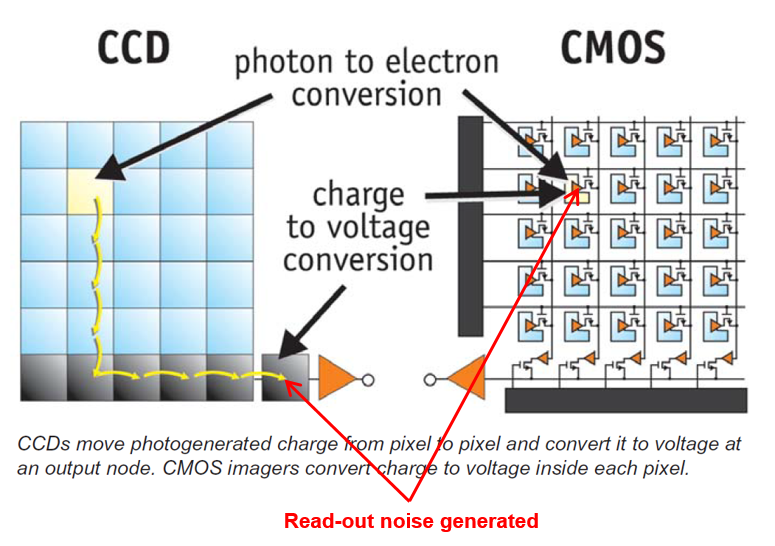
Fundamentally, both CMOS (Complementary Metal-Oxide-Semiconductor) and CCD (Charge-Coupled Device) optic architectures perform parallel photoelectric conversions—translating local photon strikes into discrete analog charges. Their elemental divergence operates entirely within the hardware read-out topology routines.
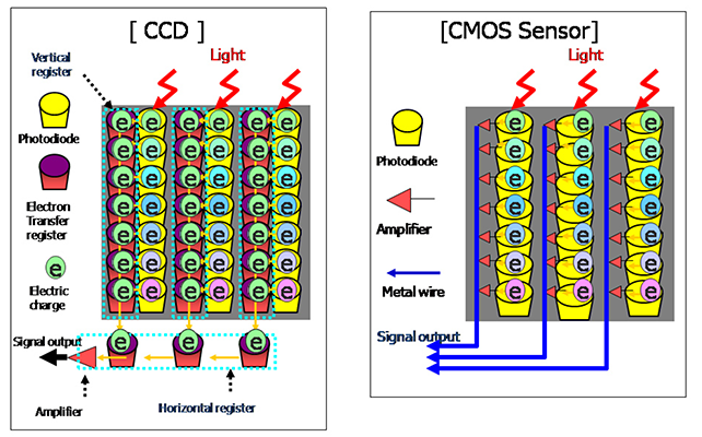
CCD arrays pipe voltage out via isolated, singular output nodes (shift registers). This maintains unparalleled continuous signal transmission without variance skew. Alternatively, localized CMOS architectures map explicit signal amplifiers adjacent to every physical sub-pixel array binding the logic natively on-site. While this sacrifices strict absolute signal uniformity, CCD nodes demand excessive high-frequency bandwidth allocations over the terminating amplifiers. Conversely, embedding parallel localized amplification vastly reduces bulk power consumption thresholds. However, managing millions of independent, localized transceivers inherently multiplies standard stationary distribution noise arrays—a classical algorithmic bottleneck for CMOS implementation topologies.
2. Physical Wafer Integration Density
CCDs trace deep origins to specialized single-crystal semiconductor manipulations. Processing these elements demands disparate synchronous circuit nodes operating on variable voltage domains (requiring distinct analog decoders/imaging processors arrayed orthogonally on the motherboard), drastically diminishing integration capacity density.
Conversely, standard CMOS components share exact fabrication profiles tied strictly to standard Integrated Circuit logic processing templates (e.g. CPU/SRAM logic construction). Because of this shared DNA, engineers effortlessly overlay local analog modifiers directly into the core matrix. A single monolithic CMOS topology binds the signal amplifier, parallel A/D (Analog-to-Digital) conversion grid, and visual ISP controller nodes. This single-die integration model precipitated the "camera-on-a-chip" era.
3. Readout Velocity Loops
CCDs operate via rigid shift-register serialization protocols—photons convert to charge packets, cascading mechanically line by line limits the ultimate frame-rate. CMOS systems harness fully arbitrary address decoders enabling localized high-speed polling vectors devoid of vertical transfer delays.
For absolute low-light forensics requiring arbitrary multi-second accumulation arrays, traditional CCD parameters eclipse standard CMOS limitations. In long-exposure routines, localized noise interference builds within CMOS registers severely corrupting data integrity.
4. EMI Noise Topologies
Historically, CCD circuits explicitly suppressed electromagnetic disruptions (EMI) via robustly embedded silicon dioxide (SiO2) PN-Junction insulators, generating impeccable raw image topologies. Because typical CMOS layers compress dense analog converters strictly beside sensitive photoreceptors, crosstalk interference heavily dictates limits. Continued algorithmic software intervention remains a necessity to cancel static interference within all high-density CMOS builds.
5. Application Constraints
CCD technology continues defining specialized high-fidelity spectrum mapping (Astro-telemetry and biological microscopy). These nodes maximize pure quantum efficiency metrics utilizing isolated dark currents limits.


Conversely, sophisticated Global Shutter CMOS implementations actively conquer high-velocity machine vision spaces mapping 3D-scanners and automation belts. Low power footprints directly tethered to independent row addresses mandate their deployment in battery-bound edge computation devices.
Source Analytics Referenced from VisionMeta