If you have arrived at this article by random means and not via its starting point, then you may find that it may not make much sense. This is because this article is one of several (six) tutorials to aid and assist in understanding the use of the ez_SIPO8_lib library in managing and controlling Serial-in/Parallel-out ICs (SIPOs) shift registers, for example 74HC595 chips.
If you wish to link to the start of the tutorial then please follow this link (Tutorial Start), otherwise, please read on...
A tutorial to consolidate understanding and use of the ez Serial-in/Parallel-out IC Library (ez_SIPO8_lib) - Tutorial 2, Relative Addressing. If you wish to link to the tutorial starting article then follow this link: Tutorial Start.
You can access and download the User Guide, Crib Sheet and the original ez_SIPO8_lib article by following these links below:
- ez_SIPO8_lib User Guide
- ez_SIPO8_lib Crib Sheet
- Read the full ez_SIPO8_lib article
Project Perspective
Shift Registers - Tutorial 2, Relative Addressing is an intuitive and flexible shift registers tutorial for relative addressing. By utilizing a 74HC595 Shift Register and 8 LEDs, you can build a more advanced electronic project and learn about basic digital logic.
Introduction to the Tutorial
In this second tutorial we will build on our Tutorial 1 experiences and look at relative addressing of the virtual SIPO output array pin pool. This form of addressing is used exclusively to address the SIPO output pins associated with 'banks' - a bank is a physical/virtual set of SIPO ICs and may represent a single SIPO IC or several (many!) connected as a cascade.
Objectives
We shall concern ourselves with creating a virtual SIPO environment in which we can apply further basic principles. In particular we shall learn:
1. how we can wire up and connect a single 74HC595 IC (SIPO) to a microcontroller, unless you have covered this in Tutorial 1
2. the structure of an Arduino sketch suitably configured to drive the physically connected SIPO IC and its LEDs, in particular:
a. creating a virtual SIPO bank
b. using relative addressing to access/update the created virtual SIPO bank
3. witness the outputs of the sketch – shifting LED patterns and serial monitor SIPO data
If you ran through Tutorial 1 and still have your components set up as for that tutorial, then skip to The Code/Sketch, otherwise continue as below.
Technical Implementation
The system uses the 74HC595 Shift Register to handle 8 LEDs using only 3 digital pins on the Arduino. This tutorial focuses on relative addressing, which allows you to set specific bits on the shift register based on their relative positions.
Hardware Infrastructure
- Arduino Uno: The primary controller for the shift register and its logic.
- 74HC595 Shift Register: This 8-bit serial-in, parallel-out chip is the heart of the LED control logic.
- 8 LEDs: Provide visual feedback on the state of the shift register.
- 220-ohm Resistors: Used to protect the LEDs and the Arduino's output pins.
- Jumper Wires: Connect all the components together.
Kit List
Gather together the following components:
- 1 x Arduino UNO - The design uses an Arduino UNO, but any suitable microcontroller (Arduino or clone) will do, providing it is able to support the pin out requirements for driving the SIPO interface and power requirements
- 1 x Breadboard - Small or large, whatever you have to hand
- 1 x 74HC595 IC - 8bit SIPO IC, or other clone providing it is genuinely ‘plug-compatible’
- 8 x LEDs - Whatever you have around
- 8 x Resistors, 220 ohm - One per LED. Use 220 ohm resisters and ignore the suggested 180 ohm values in the wiring diagrams
- Connecting wires - Short/long or breadboard wire connectors, whatever suits
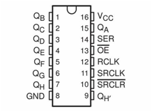
74HC595 Orientation and Pin Outs
Which end is which? Well, notice that the 74HC595 has a notch at one end, here at the top of the diagram. Pin numbering starts at 1 at the top left and continues down the left hand side and the around the bottom of the IC rising to the top right hand side to pin 16:
Microcontroller/SIPO Interface Pin Configuration
Every bank of SIPO ICs you connect to the microcontroller requires a 3-wire digital interface. The table below suggests pin mapping between the microcontroller and the SIPO IC for this tutorial, but you may choose what microcontroller digital pins you wish. If you do choose different pins then be sure to alter the sketch create_bank call.
- UNO pin 8 to SIPO pin 14 - SIPO Data Pin
- UNO pin 9 to SIPO pin 12 - SIPO Latch Pin
- UNO pin 10 to SIPO pin 11 - SIPO Clock Pin
- UNO pin +5v to SIPO pins 10, 16 - Power to the SIPO
- UNO GND pin to SIPO pins 8, 13 - Return ground (0v)
Connecting It All Together
Using the following diagram, wire up all of the components, taking care to get the output/input connections correct:
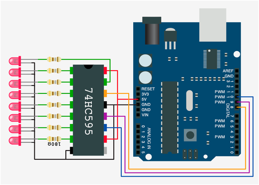
Notice that the only 74HC595 IC pin not to have anything connected is pin 9, QH’. This is used as the serial output pin to connect to the serial input pin, 14 SER, of the next SIPO 74HC595 in a cascade.
Logic and Signal Processing
The Arduino code uses the shiftOut() function to send data to the shift register.
- Clock Sync: The Arduino sets the clock pin to
HIGHand thenLOWto synchronize the data transfer. - Data Transfer: Each bit of the 8-bit value is sent serially to the data pin.
- Latch Activation: The latch pin is pulsed
HIGHand thenLOWto update the parallel output pins of the shift register.
The Code/Sketch
Now that’s done, let’s look at a sketch to demonstrate relative bank/pin addressing. This sketch will create a single SIPO bank with an output pin address range from 0–7 and a SIPO bank id of 0. As there will only be a single bank with one SIPO, the absolute address range coincides with the relative address bank range. This is always true of the first bank in any configuration but is of no consequence for what we wish to demonstrate – relative addressing using relative bank addressing functions and techniques.
The sketch will successively set up the same bank with two different 8-bit output pin patterns and update (xfer in ez speak) each to the physical SIPO IC/LEDs, in turn, with a short delay in between. The sketch then continues this repeating cycle.
Notice the two different methods used in each half of the sketch’s main loop for relative bank addressing - by individual relative bank bit and by relative bank SIPO byte (eight output port updates in one).
Using the Arduino IDE, start with a new sketch and download the tutorial sketch:
//
//   Tutorial 2 - use of ez_SPI8 library,
//   Relative addressing - 1 x physical SIPO IC
//   The sketch demonstrates two ways in which SIPO output pins
//   may be updated, individually (set_bank_pin) or in a group
//   of 8 pins (set_bank_SIPO), representing a single 8it SIPO
//   within a bank.
//
//   Ron D Bentley, Stafford, UK
//   April 2021
//
//   This example and code is in the public domain and
//   may be used without restriction and without warranty.
//
#include <ez_SIPO8_lib.h>
#define Max_SIPOs  1  // two virtual SIPOs for this tutorial
#define Max_timers 0  // no timers required
// initiate the class for Max SIPOs/timers required
SIPO8 my_SIPOs(Max_SIPOs, Max_timers);
int bank_id;  // used to keep the SIPO bank id
void setup() {
 Serial.begin(9600);
 bank_id = my_SIPOs.create_bank(8, 10, 9, 1); // absolute pin addresses 0-7, relative addresses 0-7
 if (bank_id == create_bank_failure) {
   Serial.println(F("\
failed to create bank"));
   Serial.flush();
   exit(0);
 }
 // print the bank data for confirmation/inspection
 my_SIPOs.print_SIPO_data();
}
void loop() {
 // start by setting the only SIPO (0) in the bank to all outputs off/LOW
 my_SIPOs.set_bank_SIPO(bank_id, 0, LOW);
 my_SIPOs.xfer_bank(bank_id, LSBFIRST);   // move virtual pin statuses to real SIPO output pins
 do {
   //
   // setup pattern for first cycle: 0b01010101
   // note that set_bank_pin uses relative addressing
   my_SIPOs.set_bank_pin(bank_id, 0, HIGH); // least significant bit/pin
   my_SIPOs.set_bank_pin(bank_id, 1, LOW);
   my_SIPOs.set_bank_pin(bank_id, 2, HIGH);
   my_SIPOs.set_bank_pin(bank_id, 3, LOW);
   my_SIPOs.set_bank_pin(bank_id, 4, HIGH);
   my_SIPOs.set_bank_pin(bank_id, 5, LOW);
   my_SIPOs.set_bank_pin(bank_id, 6, HIGH);
   my_SIPOs.set_bank_pin(bank_id, 7, LOW); // most significant bit/pin
   my_SIPOs.xfer_bank(bank_id, MSBFIRST);
   delay(500);
   //
   // setup reverse pattern using 8bit write function: 0b10101010
   // note that set_bank_SIPO uses relative addressing for SIPOs in the bank
   my_SIPOs.set_bank_SIPO(bank_id, 0, 0b10101010);
   my_SIPOs.xfer_bank(bank_id, MSBFIRST);
   delay(500);
 } while (true);
}
Software Execution
The code is designed to update the shift register after each state change and keep it synchronized with the overall status of the LEDs. This provides a highly responsive and engaging user interface.
Compile the sketch and upload. You should now see the LEDs ‘see-sawing’ back and forth with a small delay between cycles, as for Tutorial 1:

The result of the sketch is identical to that presented in Tutorial 1 which used absolute array addressing functions to achieve the same ends.
Notice that the first half of the above sketch looks similar to the Tutorial 1 sketch, but uses relative bank/SIPO addressing using functions set_bank_pin, set_bank_SIPO and xfer_bank, in rotation.
Which half is more efficient? Clearly the second half as this wraps up eight output pin status changes up into a single function call, which itself operates on an entire virtually mapped status byte rather than individual bits/pins.
If we wanted to be super efficient we would replace the first part of the sketch with the same function/method as for the second part, with a different SIPO byte output pin bit pattern (i.e. set_bank_SIPO(bank_id,0, 0b01010101)). Try it.
Finally, check the serial monitor, it should look like this:
SIPO global values:
pins_per_SIPO = 8
max_SIPOs = 1
bank_SIPO_count = 1
num_active_pins = 8
num_pin_status_bytes = 1
next_free bank = all SIPOs used
Number timers = 0
Bank data:
    bank = 0
    num SIPOs = 1
    latch_pin = 9 clock_pin = 10 data_pin = 8
    low_pin = 0 high_pin = 7
Future Expansion
- Daisy Chaining: Connect multiple shift registers together to control even more LEDs.
- Input Filtering: Use a shift register for input to reduce the number of pins required for