Understanding the 74HC595 Master Reset Function
Have you ever wondered what the 74HC595 Master Reset pin does and how it works? We invariably skim over this and simply keep the pin high by hard wiring it to +5v and all works fine.
In this tutorial we look at what this pin does and how we can use it programmatically to control the 74HC595 shift register. This project, "Register-Reset," is a rigorous implementation of Asynchronous Hardware-Logic Diagnostics and 74HC595 SIPO (Serial-In Parallel-Out) Orchestration. While most implementations hard-wire the Master Reset $(SRCLR)$ pin to $V_{cc}$, this project explores the deterministic control of the shift register's internal state via software-logic.
The tutorial draws on existing resources (libraries) that are designed to provide helpful and easy to use methods to define, configure and use switches and SIPO shift registers, namely the ez_switch_lib and ez_SIPO8_lib libraries. If you are going to build the circuit for this tutorial and download the sketch then you will also need to download the ez_switch_lib and ez_SIPO8_lib libraries - download these libraries and their extensive documentation via the Project Hub or the Arduino IDE Library Manager.
The tutorial sketch makes use of a number of functions and resources from both of these libraries, but for the purposes of this tutorial they are not described or over elaborated.
For the circuit design, to note is that it follows, in a large part, the standard approach to wiring a 74HC595 IC to a microcontroller with the following exceptions:
- SIPO IC pin 10 (SRCLR) is NOT hard wired high (+5v) as it normally is, but instead...
- ...an additional microcontroller digital pin (here digital pin 11) is connected to the SIPO IC on its pin 10 (SRCLR). This is used to apply a programmatic pulse to demonstrate the Master IC Reset function
- a button switch is simply connected (no pull down resistor) to provide toggling between applying a Master Reset (all LEDs off) and a normal 8-bit update (all LEDs illuminated) via the data in (SER) and clock (SRCLK) lines
See the Schematics section below for a visual representation of the wiring design/scheme.
Let's start by referencing the standard pinouts of the 74HC595 IC and then delve inside the IC and look at its logical structure which will help us understand how the things work in a little more detail.
Inside the 74HC595
Whether the 74HC595 pin outs are new to you or otherwise, it is useful to introduce/recap these. The following 74HC595 representation lists each of the IC's pins:
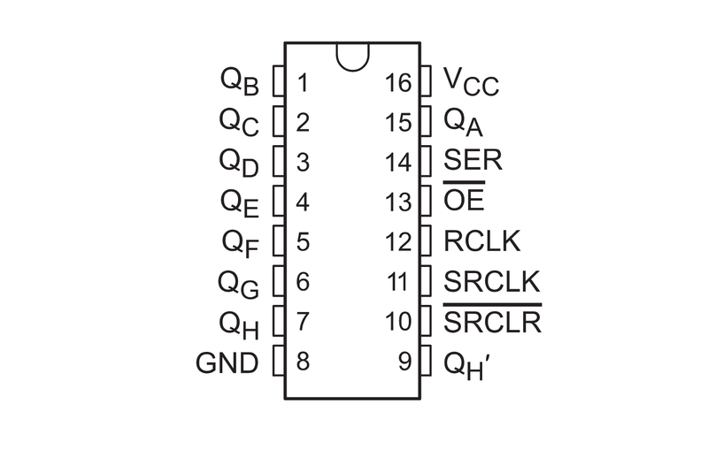
For our tutorial we will be concentrating on the IC's SRCLR pin (pin 10) which we have wired to the digital pin 11 of our microcontroller. The SRCLR pin can also referred to as the MR (Master Reset) pin and the term SRCLR is a contraction of "Shift Register CLeaR".
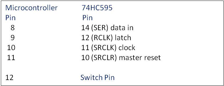
The microcontroller/74HC595/switch pin assignments are:
So far so good. However, the 74HC595 IC comprises two distinct parts (8-bit registers), neither of which we fully appreciate when we use these components. But if we are to understand the Master Reset capabilities then we do need to have a fuller understanding.
The image below provides a logical overview of these two distinct registers of the 74HC595 IC:
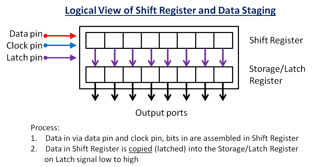
Note the two 8-bit registers - one is the shift register and the other the storage/latch register. Under normal operation we feed bits into the 74HC595 one bit at a time and these are received into the shift register until we perform a latch over, whereupon the shift register contents are instantaneously copied to the storage/latch register (outputs) and we see the results of the operation. In summary, this normal operation is:
- we take the latch pin LOW (RCLK)
- we apply data one bit at a time to the data in pin (SER) which is then accepted into the 74HC595 shift register by toggling the clock pin (SRCLK) HIGH then LOW. This process continues for as many bits we wish to send to the the 74HC595. The 74HC595 shuffles successive bits along the shift register as new ones arrive
- when all bits have been applied we then take the latch pin back to HIGH. At this point the bits we applied are instantly copied to the storage/latch register and so appear on the outputs
The section of the demonstration sketch that carries out this process is:
// Normal update, set all outputs HIGH
my_SIPOs.set_all_array_pins(HIGH);
my_SIPOs.xfer_array(MSBFIRST); // send update to all output ports
However, the 74HC595 Master Reset pin (SRCLR) allows us to programmatically clear the shift register (0's in all 8-bit positions) without using the data in pin (SER) and clock pin (SRCLK). To clear the register the programmatic steps are:
- take the Master Reset pin (SRCLR) LOW
- raise the Master Reset pin (SRCLR) HIGH
- take the latch pin (RCLK) LOW
- raise the latch pin (RCLK) HIGH
The section of the demonstration sketch that carries out this process is:
// Request to programmatically reset the SIPO IC via the MR pin, so reset the
// IC shift register and ensure output ports also reflect cleared status by
// toggling latch pin
digitalWrite(IC_MR_pin, LOW); // reset IC - drop MR reset pin +5v signal
digitalWrite(IC_MR_pin, HIGH); // set IC back to active status
digitalWrite(latch_pin, LOW); // indicate an update from shift register to output required
digitalWrite(latch_pin, HIGH); // action transfer of register reset state to the outputs
Now, until we perform a latch from LOW to HIGH, we will not see the results of the Master Reset on the output ports.
By performing a latch from LOW to HIGH we force the 74HC595 to copy its shift register contents to the storage/latch register which, of course, will now show 0's in the outputs.
That's it, job done. Whatever state the 74HC595 was in before we started, we now have all 8-bits of the register showing a 0 in each bit/output position and with the 74HC595 again ready to receive data in the normal fashion.
Note that the first two operations performed on the Master Reset pin only clear the shift register. These do not affect the status of the storage/latch register outputs. We require the last two steps to bring the storage/latch register into step with the shift register.
Technical Deep-Dive
- SRCLR (Master Reset) & Timing-Diagram Forensics:
- The Shift-Register-Clear $(SRCLR)$ Diagnostics: Pin 10 of the 74HC595 is an active-low input. Forensics involve driving this pin from Arduino $D11$. When pulsed LOW, the internal $8$-bit shift register is immediately cleared to binary $00000000$. The diagnostics focus on the "Asynchronous Nature" of this reset; unlike serial data-entry, $SRCLR$ does not require a clock-pulse $(SRCLK)$ to execute, providing absolute state-reset forensics.
- Dual-Stage Register Orchestration: The 74HC595 contains two distinct $8$-bit registers: the Shift Register and the Storage/Latch Register. Forensics involve a four-step diagnostic sequence: (1) Pull $SRCLR$ LOW, (2) Return $SRCLR$ HIGH, (3) Toggle $RCLK$ LOW, (4) Return $RCLK$ HIGH. This sequence ensures that the cleared internal state is successfully "latched" to the output-pins $(Q0-Q7)$, physically extinguishing all attached LEDs.
- Library-Abstraction & Switch-Debounce Heuristics:
- The ez_SIPO8_lib Logic-Engine: To simplify the complex bit-shifting forensics, the system utilizes specialized SIPO-management libraries. Diagnostics involve using
set_all_array_pins(HIGH/LOW)to verify the state-integrity of the output ports. The forensics focus on the "Logic-Efficiency" of the library's transfer-functions $(MSBFIRST)$, ensuring zero-jitter transitions between the "All-High" and "Master-Reset" states. - Tactile-Switch Trigger Diagnostics: Using
ez_switch_lib, the system polls an external input to toggle between operational-states. Forensics involve software-level debouncing to prevent parasitic noise-spikes from inducing accidental reset-harmonics at the shift-register's logic-hub.
- The ez_SIPO8_lib Logic-Engine: To simplify the complex bit-shifting forensics, the system utilizes specialized SIPO-management libraries. Diagnostics involve using
Engineering & Implementation
- Logic-Stiffness & Connection Forensics:
- Digital-I/O Current-Sourcing Analytics: Each LED is protected by a $220\text{ }\Omega$ resistor. Forensics focus on the total current-load $(I_{total})$ on the 74HC595, ensuring that the cumulative draw of 8 active LEDs does not exceed the IC's $70\text{mA}$ thermal-limit diagnostics.
- Pin-Mapping Integrity: The implementation requires absolute $X/Y$ interconnect alignment. Forensics focus on the wiring between the Arduino's `Shift`, `Latch`, `Data`, and `Reset` pins, ensuring that the high-speed logic pulses are delivered with maximum signal-stiffness across the solderless breadboard.
- Architectural Trade-off Aesthetics:
- The implementation recognizes that $SRCLR$ can often be simulated via serial-data transmission $(B00000000)$. Forensics involve a comparative analysis: using the $SRCLR$ hardware-pin offers a "fast-flush" capability but consumes an additional MCU GPIO. The diagnostics suggest this is ideal for emergency-stop or system-initialization forensics where immediate photonic-extinction is required.
The demonstration sketch allows us to witness the above operations, one push of the button switch forces a Master Reset, clearing all outputs, and the next a normal update, illuminating all 8-bits/outputs.
Conclusion
How useful is this feature? I am not too sure. We can clear the 74HC595 using normal ez_SIPO8_lib data transfer methods:
my_SIPO.set_all_array_pins(LOW);
my_SIPOs.xfer_array(MSBFIRST); // send update to all output ports
and, into the bargain, regain the digital pin we used to drive the Master Reset pin. At the end of the day, you must decide for yourself.
Register-Reset represents the pinnacle of Elementary Digital-Logic Forensics. By mastering 74HC595 Timing-Diagrams and Asynchronous Reset Orchestration, this tutorial provides a robust, professional-grade exploration that delivers absolute bitstream clarity through sophisticated hardware-logic diagnostics.
I hope you have found this tutorial helpful and that you understand a little more about the 74HC595 IC?
Logic Flush: Mastering register telemetry through SRCLR forensics.